The built-in MEMORY DUMP screen
The stock KN5000 firmware ships a hex memory viewer on a hidden factory screen. It can be reached on an unmodified instrument with no jumper, no jig, no disk and no power-on combination – it is a runtime chord on the panel of a normally booted machine. It reads any address in the CPU’s 16 MB space, which makes it the cheapest way to answer questions about what is really in the flash chips.
⚠ Emulator-verified, not hardware-verified. Every step below was observed in MAME and read out of the v10 disassembly. It has not yet been performed on a real KN5000. The one link that depends on the emulator is which physical cap is wired to which scan segment – see the caveats.
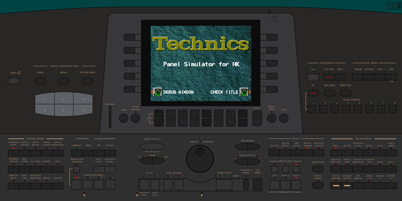
Procedure
PHYSICAL CONTROLS USED (KN5000 front panel)
- The five blank soft keys in a vertical strip at the LEFT edge of the display. Call them LEFT 1 (top) to LEFT 5 (bottom).
- The row of eight button columns directly BELOW the display (the part-volume / MUTE row). Each column has a tall UP button on top, a small MUTE button in the middle, and a tall DOWN button below. Number the columns 1 (leftmost) to 8 (rightmost).
- At the right end of that same row, a ninth pair marked PAGE (up / down).
- EXIT, the round button to the right of that row.
STEP 0 - CALIBRATION, ZERO RISK. DO THIS FIRST. Instrument on, at a normal play screen. Press and hold at the same time the UP and the DOWN button of columns 1, 6 and 8 (six caps). The SOFT VERSION screen should appear (MAIN PROGRAM / MAIN TABLE / SUB PROGRAM / SOUND TABLE - on v10 it reads 1354 / 87 / 142 / 55) and disappear again by itself after a few seconds. This is combined-word 0xA1 -> title TT_SOFTVER. If it appears, the chord mechanism is live on this unit and the column numbering used here is correct. IF NOTHING HAPPENS: our column numbering may be mirrored. Retry with columns 8, 3 and 1. If the mirror works, then everywhere below replace columns (1,5,8) with (8,4,1) and read the column list right-to-left. Do not proceed until one of the two produces SOFT VERSION.
STEP 1 - ENTER THE PANEL SIMULATOR Same idea, different columns: hold the UP and DOWN buttons of columns 1, 5 and 8 all at once (six caps). Roll them on - e.g. the three UP caps first, then the three DOWN caps - rather than slamming all six down together. The display switches to a Technics wallpaper reading ‘Panel Simulator for HK’, with the words DEBUG WINDOW at the bottom left and CHECK TITLE at the bottom right. Release everything.
STEP 2 - OPEN THE DEBUG WINDOW Press LEFT 5 (the bottom-most soft key on the left edge, next to the DEBUG WINDOW caption). A small green window titled ‘DEBUG TIME !’ opens showing -DEBUG3-.
STEP 3 - SELECT THE MEMORY DUMP Press LEFT 1 (the top-most soft key on the left edge) once. The label steps to -MEMORY DUMP- and a 16-row hex viewer appears. The menu cycles -MEMORY DUMP- / -MEMO- / -DEBUG3- and wraps, so if you overshoot just keep pressing LEFT 1.
STEP 4 - CHECK WHERE IT LANDED (SAFETY) Read the address on the first row immediately. It is whatever a DRAM variable happened to hold, so it can be anything. IF IT BEGINS WITH 1 (i.e. 0x1xxxxx), move off it at once (step 5) or press EXIT: 0x110000-0x14FFFF are the floppy controller and the main/sub CPU mailbox, and merely displaying rows there performs real, consuming reads.
STEP 5 - DIAL IN 3E0000 Each of columns 3..8 steps one hex digit of the address; UP increases, DOWN decreases: column 3 = +/- 0x100000 (leftmost digit pair) column 6 = +/- 0x100 column 4 = +/- 0x10000 column 7 = +/- 0x10 column 5 = +/- 0x1000 column 8 = +/- 0x1 PAGE up / PAGE down = +/- 0x80 (exactly one screenful) Columns 1 and 2 do nothing on this screen; that is normal, not a fault. The value wraps at FFFFFF, so any overshoot is recoverable with the same column the other way. SELF-CHECK: press one column’s UP once and watch which digit moves. If the digits respond in the opposite order to the table above, your panel numbering is mirrored - use the columns in reverse order. If UP lowers the address, use DOWN instead. The address is printed on screen, so this step is self-correcting; trust the screen over this table. SAFE ORDER: first bring the SECOND digit pair (column 4) to 0, then raise the top digit (column 3) to 3, then set column 4 to E. That keeps the address out of 0x110000-0x14FFFF while you travel. Worked example from the emulator, starting at 00F980: column 3 UP x3, column 4 UP x14, column 5 DOWN x15, column 6 DOWN x9, PAGE DOWN x1 -> 3E0000.
STEP 6 - READ AND RECORD At 3E0000, photograph the screen. The question this settles: does the row read 53 4C 49 44 45 34 4B 00 with ASCII SLIDE4K, or is it FF FF FF FF …? Our IC19 dump (sha1 4709f81…) is blank 0xFF across its whole top 128 KB (file 0xE0000-0xFFFFFF = CPU 0x3E0000-0x3FFFFF), yet v10 needs a valid SLIDE4K image there (the selector byte at 0xFFFEED is 0xFF in the v10 image, which is the ‘decompress from 0x3E0000’ branch). SLIDE4K on the real instrument means our dump is incomplete; all-FF means the chip really is blank there and the payload question moves elsewhere. While you are in there, three more cheap readings worth photographing: 0x800000 (table data, ours starts 88 00 80 00 10 2D 80 00), 0xFFFEE0 (program flash; ours reads 1B C6 03 EF 0E C2 E8 FF FF 27 0E FF FF FF 00 FF, so 0xFFFEED and 0xFFFEEF are both FF), and 0x300000 (IC19 start; ours reads 48 00 4B 00 00 00 00 00, ASCII H.K.).
STEP 7 - LEAVE Press EXIT twice. The first closes the debug window, the second returns to the normal screen. No power cycle is needed.
DO NOT CONFUSE THIS with the documented flash-write entry (load the PROGRAM DISK, hold PANEL MEMORY 1+2+3+4 at power-on, service manual page I-24). That runs Flash Memory Update and ERASES AND REWRITES IC4/IC6/IC19 - it destroys exactly the data this exercise is trying to read.
What it can read
READ: any address in the TMP94C241’s 16 MB space, 128 bytes per screenful (16 rows x 8 bytes), shown as 6-hex-digit address + 8 hex bytes + 8-char ASCII (bytes below 0x20 shown as ‘.’; bytes >= 0x80 pass through the font raw). It repaints itself about every 2 s while open, so it is a live view. Useful regions: 0x000000-0x0FFFFF work DRAM (IC9/IC10); 0x1E0000-0x1FFFFF battery-backed SRAM (IC21); 0x300000-0x3FFFFF custom-data flash IC19 - THE TARGET, with the sub-CPU payload expected at 0x3E0000; 0x400000-0x7FFFFF rhythm ROM IC14; 0x800000-0x9FFFFF table-data ROMs IC1/IC3; 0xE00000-0xFFFFFF program flash IC4/IC6. CANNOT WRITE: proven read-only with respect to the inspected address. The only access to it is an 8-byte MEM_COPY (0xFF0D99) with the user address as SOURCE; every store in 0xFA2EE6-0xFA3181 targets the local stack frame or the widget’s own 4-byte ‘adr’ variable. It issues no flash command sequence, so it cannot erase or program IC19. It also cannot export or save anything - the only output is the LCD, so this is a photograph-the-screen spot-check tool (128 bytes per screenful; ~8192 screenfuls for a whole megabyte), not a bulk dumper.
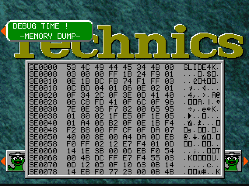
Above: the viewer in MAME pointed at custom-data flash 0x3E0000, showing the
SLIDE4K magic of the compressed sub-CPU payload. Note that in the emulator
this region is supplied by an overlay taken from a system update floppy; the
IC19 dump the project holds is 0xFF across that whole 128 KB. Reading this
address on a real instrument is exactly the measurement that would settle
the sub-CPU payload provenance question.
Caveats
- NOTHING here has been tested on real hardware. Every step was observed in MAME (kn7000-emulator build) plus read out of the v10 disassembly and ROM bytes. Felipe’s instrument is the ground truth and this needs his confirmation.
- The service manual documents NO memory-dump screen. Its Service-mode section is printed pages I-17 to I-21 (PDF pages 16-20) and lists eight diagnostics only: sub-CPU peripherals and main-CPU peripherals (CHECKING DEVICE jig on CN12/CN11), LCD test (G3+G4), CPR/CPL micro check (D3+D4 plus jig), panel switch/LED check (F3+F4), wave ROM check (E3+E4), FDC test (A3+A4), FDD save/load test (B3+B4). The chord described here is undocumented by Technics - it is firmware-proven, manual-silent.
- THE ONE MAME-DEPENDENT LINK: which physical cap is wired to which scan segment/mask. The chord is defined by the firmware in terms of soft-key subcodes 0, 4 and 7; that those are the columns numbered 1, 5 and 8 from the left comes from the project’s panel map (kn5000_cpanel.cpp CPL_SEG7..SEG10, documented as derived from the service-manual schematics). It is corroborated but not proven: in the emulator, the button MAME calls LEFT 5 opened the window whose caption the firmware itself draws at the bottom-left of the LCD, which independently confirms the left-side ordering, and the same four segments carry the column pairs in the same monotone order. If the real wiring runs the other way the chord becomes columns 8, 4, 1. The Step 0 SOFT VERSION calibration is there precisely to settle this harmlessly before anything else is attempted.
- THE SCREEN CANNOT WRITE. This is proven, not assumed: the only access to the inspected address is an 8-byte MEM_COPY with it as SOURCE, and it issues no flash command sequence, so it cannot program or erase IC19. But it is NOT side-effect-free everywhere: 0x110008/0x11000A are the floppy controller status and FIFO (a read pops a result byte), 0x120000-0x12FFFF is the FDC DMA acknowledge, and 0x140000-0x14FFFF is the inter-CPU latch IC23 whose read also clears the main CPU’s INT0. Displaying rows in 0x110000-0x14FFFF therefore performs real consuming reads 16 times per repaint, every ~2 seconds, and could desync the FDC or the main/sub CPU link until a power cycle. Not destructive to stored data, but do not park the dump there.
- The address the viewer shows when it first opens is whatever a DRAM variable holds (the widget’s ‘adr’ record, pointer in its descriptor at 0xEB31E8). It is effectively arbitrary on a given unit - check it before doing anything else (Step 4).
- The Panel Simulator is a factory screen with other windows on it (NAMING, CLIPBOARD, TRACK SWITCH, MEMO, and a full 256-entry CHECK TITLE enumerator). Only LEFT 5, LEFT 1 and EXIT were exercised. What the other controls do was not investigated - do not explore while the instrument holds data worth keeping.
- Chord timing: in the emulator, pressing both halves of column 1 on the exact same frame registered nothing, while any stagger of one frame or more always worked. That is very likely an emulator artifact of the panel HLE rather than a hardware property, but it is the reason for the advice to roll the six caps on rather than slam them. Pressing three column pairs at once may need two hands or a second person.
- UP increments the address and DOWN decrements it, by live observation. Static analysis of this routine alone reads the opposite way, so do not trust it: the firmware applies the same polarity test (bit 7 of the event code) in the memory dump and in the part-volume widget, so the button that RAISES a part volume on the home screen is the one that RAISES the address here. Either way the address is printed on screen, so Step 5 is self-correcting.
- The emulator’s reading at 0x3E0000 does NOT predict what a real unit shows. MAME overlays the compressed sub-CPU payload into the custom_data region at offset 0x0E0000 (
ROMX_LOAD("kn5000_subprogram_v14x_compressed.rom", 0x0e0000, ...), one per BIOS revision); the genuine ic19 dump the project holds is 0xFF across that entire 128 KB. The emulator run proves the viewer reads the IC19 window through the CPU bus - it says nothing about what Felipe’s chip contains, which is exactly the open question. - Throughput is 128 bytes per screenful and there is no export path. Reading the whole 1 MB of IC19 by photographing screens would be about 8192 screenfuls. This settles a question; it does not replace a dump.
- The code and the entry path are byte-identical in v7, v9 and v10, so the finding is not v10-specific - but confirm the unit’s version on the SOFT VERSION screen in Step 0 anyway.
Where it lives in the ROM
The screen is the MEMORY DUMP entry of the factory Panel Simulator screen
set (FDTest_* widgets in v10/maincpu/factory_test/fd_test_data.s), handled
by DbMemoryDumpProc at 0xFA2EE6 (v10/maincpu/ui/ui_widget_defs.s). The
entry chord is dispatched by main_title_ctrl_panel.s as
PostEvent(0x1C00015, 0x01A00000) when the firmware’s held-switch accumulator
equals 0x91. The code and the entry path are byte-identical in v7, v9 and v10.