SX-WSA1R Control Panel
SX-WSA1R — the control panel and its switch matrix
The SX-WSA1R front panel is scanned by a single Mitsubishi M37471M2196S microcontroller on the CONTROL PANEL 1 board — the same part number as the two panel MCUs in the KN5000’s control panel. Its internal mask ROM is not dumped. Everything below therefore comes from three sources that can be named: the CP1/CP2 schematic sheets of the SX-WSA1R service manual, CPU 1’s own program ROM, and measurements on the MAME driver.
Scope warning, stated up front. This page is about the rack. The SX-WSA1 keyboard’s panel is a different board — the firmware gives it two extra scan columns and three extra pots — and no SX-WSA1 document exists anywhere in these trees. Everything known about the keyboard’s panel comes from the ROM alone, which is why the emulator deliberately gives it no layout rather than a silently reused copy of the rack’s.
The wire: serial channel 1, not a dedicated port
The panel talks to CPU 1 over the TMP95C061’s serial channel 1 in I/O-interface (synchronous) mode, plus an attention interrupt and two port bits:
| line | CPU 1 pin | direction |
|---|---|---|
| TXD1 → panel SIN | P8 bit 3 | out |
| RXD1 ← panel SOUT | P8 bit 4 | in |
| SCLK1 | P8 bit 5, driven by whoever transmits | — |
| panel attention / request | INT6 | in |
| panel busy | PB bit 4 | in |
⚠ The pin names are the databook’s. What is established from the ROM is
that the SC1 module owns bits 3 and 5 of P8CR/P8FC, reads P8 bit 5 and PB
bit 4 as inputs, and will not transmit unless P8.5 reads HIGH and PB.4 reads LOW
(0xF5AB7B: bit 5,(P8) / bit 4,(PB)).
★ The panel driver is the KN5000’s, measured by bytes
Take the 3,150 bytes of CPU 1’s SC1 module (prom_b 0xF5A800-0xF5B44D) and the
whole 2 MiB of the KN5000’s v10 main program ROM, and list every common substring
of 16 bytes or more. There are eight, 154 bytes in all, and all eight land
inside the KN5000’s control-panel driver (0xFC3E65-0xFC4C33 — 3,535 bytes,
0.169 % of that ROM).
The null is what makes it a result. Run the same scan over the whole 512 KiB of prom_b against the same KN5000 ROM: 4,399 runs, 126,327 bytes — and exactly eight of them land inside the panel driver, which are the SC1 module’s eight. That is a bijection, not a cluster.
⚠ The count 8 is window-sensitive: a ninth run of ≥ 16 bytes begins at the module’s last byte and ends exactly at the panel driver’s first byte. It is recorded here rather than quietly trimmed away.
Reproduce: wsa1_kn5000_panel_bytediff.py (the module scan) and
wsa1_panel_report_refutation.py --selftest (the null), both in
kn7000_mame/notes/wsa1-probes/.
The correspondence is routine for routine, at the same offset inside the routine, and the two packet dispatchers are the same instruction with a different table pointer — ten bytes of which three differ, the low three bytes of the 32-bit immediate:
WSA1  0xF5B0AB: eb c8 b5 b0 f5 00 a3 23 b3 d8   add XHL,SC1_RxOpTable
KN5K  0xFC4959: eb c8 65 49 fc 00 a3 23 b3 d8   add XHL,CPanel_RX_PacketHandlers
Both tables even have the same shape and grouping — RX 8 entries
([0][1] button, [2] analogue, [3][4][5] sync, [6][7] multi-byte), TX 4
entries — and the delay constants match: SC1_WaitTicks2 / SC1_WaitTicks6 /
SC1_WaitTicks51 against the KN5000’s DELAY_2_TICKS / DELAY_6_TICKS /
DELAY_51_TICKS.
⚠ The counter-example that keeps this honest. Elsewhere in the same pair of
machines, DSP_WriteChannelRegs_Inner is 80 of 81 bytes identical to the
KN5000’s — and the one differing byte is the peripheral base. Always diff the
bytes before reusing a name.
The switch matrix: 58 populated cells
The M37471M2196S drives SEG0..SEG10 as scan columns and reads SW0..SW7 as return rows. On the rack:
- SEG6 (pin 40) and SEG10 (pin 33) are dead stubs — they stop 35 px past the package edge at 400 dpi, which is the pin-number underline, not a wire. Nine of the eleven strobes survive past that point. Those two segments exist for the keyboard variant.
- 58 cells are populated: 47 on CP1 and 11 on CP2, matching the parts-list counts exactly, with a single hole at SEG2/SW7 (SW24 / D24 not fitted).
The trace was done by programmatic black-run extraction on a 400 dpi render of
the CP1/CP2 P.C. Diagram (manual II-29/30) — wsa1_sch_hscan.py,
wsa1_sch_vscan.py and wsa1_sch_crop.py, with the coordinates and the joins
written out in wsa1_sch_TRACE.md so anyone holding the manual can re-check
every net claim.
An independent cross-check inside the schematic itself: the six SEG lines that carry LEDs are exactly {0, 1, 2, 3, 8, 9}, and exactly those six are buffered by IC3’s (HD74LS07P) six open-collector gates; {4, 5, 7} carry switches only and go straight from IC1. A hex buffer with six LED-bearing columns is not a coincidence, and any off-by-one in the column mapping breaks the pattern.
★ A second witness, from the ROM, that never saw the schematic
prom_a carries its own variant-2 switch → LED adjacency table at 0xF95088,
which stores 0x0000 for a position with no switch. Relabel its nine rows as the
nine wired segments and its zero pattern is the schematic: the same 58
populated cells, the same hole at SEG2/SW7, the same 11-vs-9 segment count.
kn7000_mame/notes/wsa1-probes/wsa1_sch_vs_rom_matrix.py reports FAILURES: 0, and nothing from the
schematic was fed into that script — so it is a genuine second witness to
segment ↔ column, bit ↔ row and population.
Provenance per button
All 58 switches now have a legend and a (segment, bit), and each carries the
tier of evidence it rests on:
| tier | count | how the legend was obtained |
|---|---|---|
| [L] | 29 | the CP1/CP2 P.C. Diagram prints the legend beside the switch |
| [B] | 19 | net traced; panel position read off the P.C. BOARD page (II-27/28), whose orientation is fixed in both axes by silkscreen — the keypad reads 7, 8 left-to-right and 7/4/1/0 top-to-bottom, and PAGE is silkscreened up on SW22, down on SW21 |
| [F] | 10 | the ten LCD soft keys: net traced like tier B, but the left/right column reading came from the firmware — see below |
The complete map as the emulator declares it:
| segment | bits 0–7 |
|---|---|
| SEG0 | PLAY MODE SOUND · PLAY MODE COMBI · EDIT MODE SOUND · EDIT MODE COMBI · BANK USER 1 · BANK USER 2 · BANK ROM/EXT · BANK RE-MAP |
| SEG1 | number 0 · 1 · 2 · 3 · 4 · 5 · 6 · 7 |
| SEG2 | number 8 · number 9 · +/− · ENTER · PAGE down · PAGE up · COMPARE · (not fitted) |
| SEG3 | LCD soft key RIGHT 1–5 · −1 · +1 · EXIT |
| SEG4 | under-LCD keys, columns 1–4, bottom/top alternating |
| SEG5 | under-LCD keys, columns 5–8, bottom/top alternating |
| SEG6 | keyboard variant only — dead stub on the rack |
| SEG7 | MENU PART · MENU SYSTEM · MENU MIDI · MENU DISK · (four not fitted) |
| SEG8 | REALTIME CREATOR 1~6 · REALTIME CREATOR RESET · (six not fitted) |
| SEG9 | LCD soft key LEFT 1–5 · (three not fitted) |
| SEG10 | keyboard variant only — dead stub on the rack |
★ The firmware settled the soft-key columns
Neither five-key column beside the LCD is legended on either board, and both
carry the ROM’s family tag 0x0604, so only the board page’s left-right
orientation separated them — the one reading that a photograph of a real rack
could still overturn. Screen 0x40, the DISK menu, draws four entries down
the left of the LCD and two down the right. Pressing rows 1..5 of each column
and reading the screen the firmware moves to gives:
| row | SEG9 | SEG3 |
|---|---|---|
| 1 | 47 DISK LOAD |
54 LOAD SINGLE SOUND |
| 2 | 4C DISK SAVE |
53 LOAD SINGLE COMBI. |
| 3 | 45 MIDI FILE DIRECT PLAY |
40 no change |
| 4 | 50 FLOPPY DISK FORMAT |
40 no change |
| 5 | 40 no change |
40 no change |
Four live rows on SEG9 and two on SEG3 — exactly as the menu is drawn. SEG9 is
the LEFT column. Reproduce with
kn7000_mame/notes/wsa1-probes/wsa1_softkey_columns.sh.
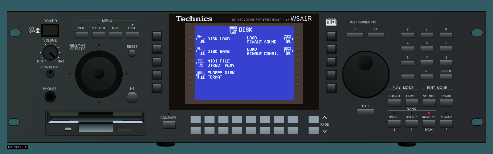
0x40 and lights the DISK lamp — four entries down the left of the LCD, two down the right. The machine is MACHINE_NOT_WORKING | MACHINE_NO_SOUND.The lamps
There are 18 lamps on the rack, and prom_a’s table at 0xF95088 names 14 of
them outright. The word stored there is (LED register << 8) | LED bit mask —
confirmed from the instructions rather than assumed: sub_F94E1C does
ld WA,(XHL) and calls 0xF40670, which reaches the unguarded entry of the LED
register writer at prom_a 0xF8C846, mapping W through the register → wire
table and queueing [wire][A]. So the high byte is the register and the low byte
is the data. kn7000_mame/notes/wsa1-probes/wsa1_lamp_identification.py reports
FAILURES: 0.
★ The LED output space is 47 wide, not 64 — and that is a measurement
The emulator exposes 64 LED outputs, led0..led63, because the register file
is 8 registers × 8 bits. Only 47 of them are lamps anywhere on this machine.
The PANEL SW&LED CHECK’s all-on sweep (sub_F956B0, prom_a 0xF956B0) walks
the word table at 0xF95C68 until 0xFFFF, and that table is exactly
reg0=FF reg1=FF reg2=FF reg3=FF reg4=FF reg5=03 reg6=0F reg7=02. At the
driver’s index register × 8 + bit, the seventeen outputs the firmware’s own
test never lights are led42-47, led52-56 and led58-63 — and they are
recorded in wsa1_cpanel.h so that no layout ever wires a lamp to one of them.
(That 47 is the whole output space across both variants; the rack’s own panel
drawing carries 18 lamps, of which 14 are named by the ROM table above.)
What makes 47 a measurement rather than a reading: the union of every mask in the
two switch → LED adjacency tables (0xF94F58 variant 1, 0xF95088
variant 2) is a subset of that sweep, register by register. Two unrelated
tables agree.
⚠ A near-miss worth recording: those adjacency tables carry their own wire →
segment maps (0xF94ED8 / 0xF95008), and they are not byte-identical to
the ones the driver already uses (0xF8A109 / 0xF8A189) — they are those maps
minus the 0xD0-block analogue wires (five for variant 1, two for variant 2).
Over the switch segments 0xC0..0xCA they agree exactly, including the 11-vs-9
count and the 0xC6/0xCA absence, so the corroboration is real — but the word
“exactly” would have been wrong.
Drawn but not bound, and why
| control | why it has no binding |
|---|---|
| the four REALTIME CREATOR ring lamps | the ROM pins the set to {led16, led17, led24, led25} (RESET lights register 2 mask 0x03, “1~6” lights register 3 mask 0x03) but not which is north/east/south/west |
| the floppy activity lamp | it belongs to the drive; the driver exposes no output for it |
| CONTRAST | VR2 on CP2 is an LCD bias pot whose wiper returns to MAIN as VO. It is not a panel-MCU input, so there is no port to bind |
| POWER, PHONES, floppy eject | no port exists for any of them |
| REALTIME CREATOR itself | it is not a panel control: it is board MB2’s triple-gang VR2, reporting JOYX/JOYY to a TMP95C061 A/D. Drawn, and inert |
The analogue wires
The panel link carries continuous controls as “wires” in the 0xD0 block, each
with its own transfer curve in prom_a:
| wire | curve | entries | shape | present on |
|---|---|---|---|---|
0xD0 |
0xF89C34 |
128 | monotonic, no plateau | variant 1 only |
0xD1 |
0xF89CB4 |
256 | 18-entry plateau at 0x80, its midpoint |
variant 1 only |
0xD2 |
0xF89B34 |
128 | 13-entry plateau at 0x40, its midpoint |
variant 1 only |
0xD3 |
0xF89AB4 |
128 | monotonic, no plateau | both |
0xD7 |
(the data-entry encoder) | — | — | both |
Two centre plateaus, not one: 0xD1 and 0xD2 are both centre-detented,
i.e. sprung bipolar controls — which is part of the corroboration that variant 1
is the keyboard. ⚠ An earlier claim that only 0xD1 had a dead zone was
false, and is corrected here. When the strap says variant 2, the gate
substitutes 0xD0 → 0x00, 0xD1 → 0x80, 0xD2 → 0x40 — a minimum and two
midpoints — while 0xD3’s handler at 0xF89A8B has no (0xC4) test at all,
because that control is present on both machines.
⚠ Also refuted: the two “software analogue channels” that variant 2 keeps in the
0xF8DC25 scan are not controls. sub_F8DD4D and sub_F8DD62 read RAM
(0x600000) / (0x600001), which are parked at 0x80 and written by prom_b’s
display-list interpreter.
⚠ And the address byte’s bits 7:6 are not a panel identity. Six prom_a
callers pass W = 0, 1, 2, 3, 4, 5 — the on-CPU A/D channels, i.e. bank 00 of
the same dispatcher — so bits 7:6 select the source (00 = on-CPU A/D,
11 = the panel link), and nothing in either ROM ever compares them against a
constant.
Power-on chords, and the two ways into service mode
Three chords are read from the panel’s own change-mask shadow at RAM
0x2B20 + ((wire & 0x0F) | ((wire & 0x40) >> 2)):
| chord | variant 1 | variant 2 | effect |
|---|---|---|---|
| ROM version display | seg 2 bits 0–2 (0xF82952) |
seg 0 bits 4–6 (0xF8295F) |
shows the version on the LEDs |
| FACTORY CLEAR | seg 8, (0x2B38) == 7 exactly (0xF828DF) |
seg 8 bits 0–1 (0xF828E9) |
zeroes RAM, writes 0x5AA5 at 0x7FCA, jumps to RESET |
| third service entry | seg 10 bits 5–7 (0xF82A0A) |
seg 3 bits 5–7 (0xF82A18) |
not identified |
On the rack: the number pad
sub_F953CD (prom_a) — reached once from RESET at 0xF827F8 → 0xF40148 →
0xF952FC, and only when the strap says (0xC4) == 2 — compares (0x2B31),
which is wire 0xC1 = SEG1, for equality:
| SEG1 bit | value | screen | title |
|---|---|---|---|
| SW1 | 0x02 |
— | recognised, falls through without setting a screen |
| SW2 | 0x04 |
0xD9 |
PANEL CPU CHECK |
| SW3 | 0x08 |
0xDA |
SINE WAVE CHECK |
| SW4 | 0x10 |
0xDB |
PANEL SW&LED CHECK |
| SW5 | 0x20 |
0xDC |
the automatic screen cycler |
⚠ Equality, so a second button held in SEG1 kills it. And the RESET block
tests four chords in address order, where the ROM-version arm at 0xF8294C
never returns — so a held ROM-version chord pre-empts a service screen this
test has already latched.
★ On the keyboard: from the keybed, which no sibling machine does
On the (0xC4) == 1 arm, sub_F9530B does a link remote read of eight bytes
from CPU 2’s 0x0000FFF0 and does nothing unless exactly two bits are set
(cps L,0x02 / jrl NZ at 0xF95346).
0x0000FFF0 is CPU 2’s 61-key state bitmap: KeyScan_InitKeyStateBitmap
(prom_c 0xF9988D) clears eight bytes there and folds scanner events in at byte
(key >> 3) & 7, bit key & 7. ★ That closed an open question in the
disassembly, which had looked for a consumer of the bitmap in prom_c and found
none: the consumer is on the other processor.
The five bit pairs are all exactly twelve keys apart — a self-check on the
bit → key decode that could have failed and did not — so every chord is the same
note an octave apart. Key 0 is MIDI 36, the firmware adding 36 inside
ToneGen_VelocityFromTouch (prom_c 0xF995EC):
| chord | keys | screen | title |
|---|---|---|---|
| C4 + C5 | 24, 36 | — | recognised and rejected (0xF95359) |
| D4 + D5 | 26, 38 | 0xD9 |
PANEL CPU CHECK |
| E4 + E5 | 28, 40 | 0xDA |
SINE WAVE CHECK |
| F4 + F5 | 29, 41 | 0xDB |
PANEL SW&LED CHECK |
| G4 + G5 | 31, 43 | 0xDC |
the screen cycler |
★ The decode is confirmed live, against a criterion that could have failed.
Holding D4 + D5 from t = 0 on the wsa1 driver, CPU 2’s bitmap reads
00 00 00 04 40 00 00 00 — popcount 2 — steadily from t = 5 s: byte +3 bit 2
is key 26 = D4 and byte +4 bit 6 is key 38 = D5, exactly the pair sub_F9530B
tests for screen 0xD9.
⚠ And the chord still does not fire in the emulator: RAM (0x2070) is never
written with 0xD9. That localises the failure to CPU 1’s side of the remote
read and rules out the two other candidates — the bitmap is not empty, and
nothing pre-empts a screen that was never requested. The live hypothesis is
ordering: CPU 1 asks at 0xF827F8, before even its own 0x384-tick wait,
while CPU 2 does not build the bitmap until 0xF997FA, and until 0xF9816B
moves XSP those eight bytes are CPU 2’s boot stack. Not proven — the remote
read could simply be failing. The chords are documented because they are
established, not because they work.
The bug that made every button inert — and how it was found
Until 2026-08-26 no panel button on this machine had ever done anything, and the
receiver looked wrong: a press of wire 0xC1 stored 0xC1 at index 0 instead of
the value byte at index 1.
None of the three obvious candidates was to blame — not the byte count, not
the length rule, not the ring index. What was wrong was when the panel asked.
INT6_SC1_PeerRequest (prom_b 0xF5AC0A) reads an INT6 that arrives while a
frame is in flight as “the peer is re-synchronising” and rewinds the receive
ring by one byte (decw 1,(0x2A92) at 0xF5AC4A), expecting a re-send. The
emulated panel’s attention line was an invented 50 µs pulse repeated every 2 ms
until the CPU accepted, and it pulsed straight through CPU 1’s own opening
transmits.
Measured before (wsa1_sc1_ring_phase.lua): three such edges at
t = 0.326 / 0.334 / 0.342 s walk the write index 0000 → 004C → 0049 while the
read index is still 0000; the reader then chews 27 empty slots, meets the
writer at 004A with odd parity, and from then on pairs the previous
message’s data byte with this message’s address byte for the rest of the
session.
Measured after the panel HLE stopped asserting attention during a frame:
read index == write index == 0x0006, sync answers dispatched through
SC1_RxOp3_Discard instead of being chewed, and —
| press (through the layout’s own binding) | shadow while held | screen | lamps |
|---|---|---|---|
MENU DISK, SEG7 0x08 |
(0x2B37) = 08 |
01 → 40 (the DISK menu) |
led8 off, led41 on |
BANK USER 1, SEG0 0x10 |
(0x2B30) = 10 |
01 → A1 |
led0 on, led2 off |
PLAY MODE COMBI, SEG0 0x02 |
(0x2B30) = 02 |
01 → 02 |
led9 on, led8 off |
— the exact bit, the right screen, and the lamp the schematic says belongs to that button.
★ The instrument mattered as much as the fix. “Did an LCD write happen” is
the wrong probe for a panel press: 459 of the 654 dispatch-matrix handler
slots are 0xFF42B1, a bare ret, so most positions doing nothing on the play
screen is expected. Probing the chain instead — 0x2B20..0x2B3F (did it reach
CPU 1) → 0x2082 (control byte) → 0x2070/0x2071 (was a screen requested) →
0x207C (is the dispatcher there) — is what turned the bug up.
The screen objects: how a screen is dispatched
A screen request resolves through the screen-object table
PanelScreen_VtableTable (prom_a 0xF86EC1) — 256 little-endian pointers, one
screen object per slot, each object a three-method vtable: +0 ENTER (paints
the screen), +4 LEAVE, +8 BUTTON. The offsets are pinned by their callers,
not guessed: +0 is invoked with the id that has just become current, +4 with
the id that just stopped being current, and +8 by PanelButton_Route
(0xF8621E) with the current id and a button index. A screen id n addresses
entry n + 32: PanelButton_Route reads the table through a second base,
PanelScreen_VtableTable_ViewB at 0xF86F41 (= 0xF86EC1 + 0x80), so the id
space and the raw table index differ by 32.
81 of the 256 slots point at the shared stub PanelScreen_NullVtable, whose
three offsets all reach one ret — an unpopulated screen. The remaining 175
live objects are every screen this instrument has: the MODELING tone-editor
pages, SOUND MODE, the service screens, and the whole disk-menu family all sit
here. A button press therefore resolves as screen id → object → BUTTON method,
and the same object’s ENTER method is what paints that screen.
The DISK menu closes on itself, which is a check on the whole mapping. The menu
(screen id 0x40, object entry 0x60) is itself a menu of
PanelScreen_VtableTable ids: each LCD-row key writes one of the other disk
screens’ ids into the screen-request cells (0x2070)/(0x2071), and every id it
can write is one of the nine disk screens the same module owns.
⚠ This names the mechanism, not every screen. Of the 175 live objects, 32
carry a named ENTER method in prom_a and 36 have their ENTER in prom_b; the ENTER
methods of about a hundred screens are still sub_XXXXXX, because most delegate
their drawing to a helper rather than painting text inline, so a screen’s title
is two or three calls away from its object. Naming one ENTER method names that
screen’s LEAVE and BUTTON methods for free. Reproduce the table and its method
offsets with wsa1/notes/prom_a_naming_wave8_apply.py --screens and
wsa1/notes/prom_a_screen_methods_wave29.py.
What is still open
- Which of the four REALTIME CREATOR ring lamps is which. The set is pinned; the order is not. The layout draws all four and binds none.
- The whole SX-WSA1 keyboard panel. Different board, two extra scan columns, three extra pots, and no document. Its emulator ioports stay positional.
- The
(segment, bit) → control indexmap at0xF869F0-0xF86A23. That is the dispatch side rather than the identity side, and resolving itsXIX/XIYwould turn all 88 positions into dispatch-matrix slots. It is the highest-value next step. - A better scan of the self-diagnostic pages. They map the wave-ROM tests
onto buttons, and the OCR loses the circled digits. ⚠ It is seven tests,
not six:
0xF95971readsH = (0x2267) & 0x0Fand rejectsH < 1andH > 7, so the circled digits are (1)..(7) on a numeric entry rather than seven separate buttons.
The layout itself
src/mame/layout/wsa1r.lay is generated, not hand-drawn, by
tools/gen_wsa1r_lay.py from Felipe’s SVG artwork reproducing the manual’s
ARRANGEMENT OF CONTROL PANEL page. Every <bounds> comes from
tools/wsa1_svg_geometry.py, whose self-test pins nine landmarks — the LCD among
them, drawn 1:1 at exactly 320 × 240. Do not hand-edit it: edit the SVG or the
generator and re-run.