SX-WSA1 / SX-WSA1R
Technics SX-WSA1 / SX-WSA1R — the acoustic-modelling synthesizer
The Technics SX-WSA1 (keyboard) and SX-WSA1R (rack module) are a 1995 pair of “ACOUSTIC MODELING SYNTHESIS” instruments — not arranger keyboards. The specification page has no rhythm, style or auto-accompaniment row at all: this is a 64-note, 32-part synthesizer built around a “MODELING LSI”, with a floppy drive and two sets of MIDI ports. They are the first non-arranger machines documented on this site, and they are here because they turn out to share both silicon and literal machine code with the KN5000.
Status: early, and honest about it. Both variants are declared in a development MAME driver that boots them to their real
SOUND MODEscreen and takes button presses. It makes no sound at all — the tone generator and the three DSPs are not modelled, and all six wave mask ROMs are undumped. Since 2026-09-01 the modelling window at0x00104000has a placeholder device that models its register interface and synthesises nothing. A byte-exact disassembly of all four EPROM images exists; every one rebuilds from source with no.incbinat all, and 78.2 % of the 2,097,152 bytes is substantive source, the remainder being verified uniform filler (wsa1/scripts/analysis/source_coverage.py). See Emulation Status and Disassembly.
⚠ Provenance: these images are not dumps this project made
Nobody working on this driver has read an SX-WSA1R EPROM. The four firmware
images are the publicly circulated “v2” OS set, downloaded in August 2026 from
the synthesizer-preservation site dbwbp.com (also mirrored on archive.org) and
recorded in technics_roms/roms/wsa1/PROVENANCE.md. The uploader states the set
was read from a rack SX-WSA1R and works unmodified in the keyboard SX-WSA1 —
that claim is the only basis for running the same images in both drivers, and
no SX-WSA1 material exists in these trees to check it against.
They are declared without a dump-quality flag because nothing suggests the bytes are wrong: what is second-hand here is the provenance, not the integrity. Four mutually independent checks agree —
- each image is exactly 524,288 bytes, the 256K × 16 organisation the service manual’s block diagram draws for the program EPROMs;
- three of the four end with their own build tag (
wsaa_822,wsac_230,wsad_54), matching the AX / CX / DX endings of the factory part numbersQSIGCWSA1AX,QSIGCWSA1CX,QSIGCWSA1DXprinted in the manual; - the firmware’s own
ROM VERSIONscreen has exactly three slots, labelledWSA-A:,WSA-C:andWSA-D:— and the one image carrying no build tag is precisely the one the screen has no label for; - the A and C images each carry a TLCS-900/H vector table in their last 256
bytes — 33 of 64 words point into
0xF00000-0xFFFFFF, where a TMP95C061 fetches its reset PC, against 3 and 0 for the other two images, which serve as the negative control.
“v2.0” is the name the set circulates under. It appears in neither the service manual nor in any of the four images; the only version strings the firmware carries are those three build tags.
Everything about the rack rests on the SX-WSA1R service manual (ORDER NO. EMID951604, © 1995 Matsushita Electric Industrial), whose scan available here is photocopy grade. There is no SX-WSA1 service manual anywhere in these trees — everything known about the keyboard variant’s panel comes from the ROM alone.
At a glance
| Property | SX-WSA1 / SX-WSA1R | (KN5000 for comparison) |
|---|---|---|
| Year | 1995 | 1997 |
| Category | acoustic-modelling synthesizer, keyboard + rack | arranger keyboard |
| CPUs | two Toshiba TMP95C061AF (TLCS-900/H), IC1 “MAIN” + IC2 “SUB” | TMP94C241F (TLCS-900/H2) main + sub |
| Clock | fc = 28 MHz, both parts (derived from the firmware) | 25 MHz |
| Polyphony | 64 notes, 32 parts max. | — |
| Sounds | PRESET 256 + 16 drum kits, 128 combinations; USER 256 + 4 kits, 128 combinations | — |
| Effects | DIGITAL EFFECT 12 types; DSP EFFECT 44 types + REVERB 12 types | 50-effect DSP catalogue |
| Display | SED1330FBA, 320 × 240 dot monochrome LCD | 320 × 240 colour, VGA-style controller |
| Storage | 3.5″ floppy, 2HD 1.44 MB / 2DD 720 KB, uPD72070 FDC | 3.5″ floppy, uPD72067 |
| MIDI | MIDI IN / OUT / THRU × 2 | single set |
| Program ROM | four 4 Mbit EPROMs (2 MB total), IC12/IC13/IC28 + the D image | 2 MB main + 192 KB sub payload |
| Kernel | custom TLCS-900 RTOS, the same one on both CPUs | the same RTOS lineage (see below) |
| MILK UI framework | absent | absent (it arrives with the MN10300 models) |
Rack dimensions 48.2 × 14.1 × 25.2 cm, 6.5 kg; accessories AC cord, DEMO DISK and a MIDI cable. Rear panel: PHONES, MAIN OUT (R, L/MONO), SUB OUT (R, L/MONO), MIDI IN/OUT/THRU × 2. (Specification page of the SX-WSA1R service manual.)
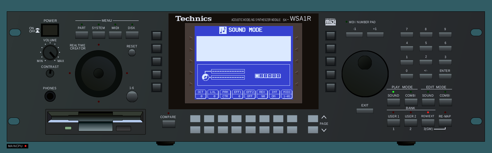
SOUND MODE screen at t = 45 s. The panel artwork is Felipe's own SVG redrawing of the manual's ARRANGEMENT OF CONTROL PANEL page; the LCD content is the firmware's. The machine is MACHINE_NOT_WORKING | MACHINE_NO_SOUND — it makes no sound.Two products, one ROM set, one strap bit
Technics shipped the same firmware in two boxes and let the board tell the
firmware which one it is in. The detection is established from the ROM:
prom_a 0xF82882, reached once from RESET at 0xF827D8, is exactly
ld A,0x01 / bit 0,(PB) / jr NZ,+2 / ld A,0x02 / ld (0xC4),A / ret
and it is the only write to RAM (0x0000C4) in 512 KiB. PB bit 0 is an input:
RESET writes PBCR = 0x0C, making only bits 2 and 3 outputs, and PBCR is
written exactly once in either image. 111 well-formed cp (0xC4),#imm / jr cc
sites in 27 distinct 4 KiB blocks read the answer back, and every one of them
compares against 1 or 2 and nothing else.
The shape is unique: no other CPU-1 direct-page byte has ≥ 20 tests and ≤ 1
producer. The neighbour that validates the decode is (0xC5), the expansion-board
flag — same idiom, five instructions away, set to 0x5A at 0xF828C3 after
comparing ten bytes read from CPU 2’s 0xC00000 against the ROM string
WSA1 EXTBD.
What the two arms actually do, each read out of the disassembly rather than guessed:
| site | (0xC4) = 1 |
(0xC4) = 2 |
|---|---|---|
0xF8DC25 |
scans all four of CPU 1’s A/D channels | skips all four (first skipped call 0xF8DC3E ld WA,(0x60); SFR 0x60 is ADREG0L) |
0xFF42EE |
display list 0xF580B0 — MIDI FILE LOAD / MIDI FILE SAVE / LOAD SINGLE SOUND / LOAD SINGLE COMBI. |
display list 0xF58127 — only the last two |
0xF8A109 / 0xF8A189 |
11 button segments + wires 0xD0 0xD1 0xD2 0xD3 0xD7 |
9 segments + wires 0xD3 0xD7 |
0xF8C8AC / 0xF8C8B7 |
LED-register → wire map, variant 1 | variant 2 |
★ Which arm is which model is corroboration, not decode
No string in any of the four images names either model. The assignment
“(0xC4) = 2 is the rack” rests on two independent readings of the rack’s own
manual, and it is stated that way here on purpose:
- the specification page’s disk menu has no MIDI FILE LOAD and no MIDI FILE SAVE, matching the shorter display list; and
- the mechanical parts list has one VOLUME KNOB and one DIAL WHEEL and no
bender, matching the one pot (
0xD3) and one encoder (0xD7) that variant 2 keeps — where variant 1 additionally carries0xD0,0xD1and0xD2, two of which have centre-detented curves (an 18-entry plateau at0x80in the 256-entry table at0xF89CB4; 13 entries at0x40at0xF89B34), i.e. sprung bipolar controls a rack module does not have.
⚠ Even so, the surviving evidence establishes only that the (0xC4) = 2 machine
reads none of CPU 1’s own A/D channels, carries one pot and one encoder on the
panel link, and has a shorter disk menu. That is consistent with a rack and it
does not exclude any other build without that panel board. A third “match”
— reading the specification’s OTHERS VOLUME, DATA ENTRY DIAL/KEYS, COMPARE row
as a count of continuous controls — was claimed and is withdrawn; it is an
others row and it is not evidence.
What would settle it: an SX-WSA1 service manual or parts list, a photograph of either machine’s CN-numbered panel connector, or a ROM set whose display lists differ.
⚠ Three related claims were refuted and must not come back: the strap does
not gate the keybed (there is not one cp (0xC4) anywhere in
0xF8E000-0xFFFF, and prom_c contains no PB read at all); CPU 1 is not “refusing
keybed traffic because it decided it is a rack”; and P5 bit 4 is not a model
strap — it is the service CHECKING DEVICE’s switch, and the manual says so.
Hardware
Everything below is the SX-WSA1R service manual’s parts list and schematic sheets, read at 400 dpi. The scan is photocopy grade: several part numbers print differently on the schematic and in the parts list, and a number of reference designators did not survive at all. Where the two disagree both readings are recorded; where a designator is derived rather than read, it says so.
Main board
| Ref | Part | Role |
|---|---|---|
| IC1 | TMP95C061AF | Toshiba TLCS-900/H, “MICROCOMPUTER (MAIN)” |
| IC2 | TMP95C061AF | Toshiba TLCS-900/H, “MICROCOMPUTER (SUB)” |
| IC3 | L7A1429 | “MODELING LSI” — the engine the machine is named after: 64 channels of coupled linear resonators, nineteen 16-bit parameter registers each. A MAME device (l7a1429_device) models the register interface at 0x00104000; it synthesises nothing. ⚠ That 0x104000 decodes to this part is an inference — no ROM names a part number — so the disassembly still calls it Dev104_. Full account: Acoustic Modelling LSI. |
| IC4 | TC183C230002 | “TONE GENELATOR LSI” [sic] |
| IC30 (+ two more) | NEC uPD6383GF-3BA | three digital signal processors — the same part as the KN5000’s IC311. ⚠ Only the IC30 designator prints cleanly; the other two schematic instances read as IC5 and IC6, and the block diagram shows three DSP blocks, so three is the count used |
| IC7 | SED1330FBA | LCD controller for the 320 × 240 dot panel |
| IC12 / IC13 | QSIGCWSA1AX / QSIGCWSA1BX |
4 Mbit programmed EPROMs, chip selects PROMACS / PROMBCS |
| IC28 | QSIGCWSA1CX |
4 Mbit programmed EPROM, chip select PROMCCS |
| (designator not asserted) | QSIGCWSA1DX |
4 Mbit programmed EPROM, chip select PROMDCS. The designator column is missing from both places this part is printed; the redistributed file is named .ic21 and the parts-list row order agrees, but nothing in the scan available here confirms it |
| (designator not asserted) | AM29F400T | 4 Mbit flash — same situation; the parts-list row order puts it at IC22 |
| IC27 | D74HC139GS | decoder; generates PROMCCS and PROMDCS |
| IC43–45, IC47–49 | QSIGH3C16* |
six 16 Mbit wave mask ROMs — all undumped. There is no IC46 in either the parts list or the self-diagnostic |
| IC52–54, IC59 | PCM1702U | four D/A converters |
| IC55–58 | M5218AFP | operational amplifiers |
| IC14 / IC15 | M5256CFP70LL / M5M44170AJ7S | 256 kbit static RAM, 4 Mbit DRAM |
| IC23, IC31, IC32, IC51, IC61 | LC321664AJ80 | 1 Mbit DRAM |
| IC33, IC34 | M5M44260AJ7S | 4 Mbit DRAM |
| IC71 | LH5P832N-10 | 256 kbit RAM (schematic: pseudo-static; parts list: static) |
| (unknown) | uPD72070GF3BE | NEC floppy disk controller, for the 3.5″ 2HD/2DD drive |
Control panel 1 board
| Part | Role |
|---|---|
| M37471M2196S | Mitsubishi panel microcontroller — the same part as the two MCUs in the KN5000’s control panel. Internal mask ROM not dumped; no ROM region is declared for it because the manual does not give its capacity. |
| HD74LS07P | hex buffer |
⚠ The tone-generator identity is corroborated, not settled. The parts-list OCR
prints it both as TC183C230002 — which would match the KN5000’s IC303 — and as
TC1830230002, differing in one character (C against 0), which is the
confusion this scan makes most often. PROVENANCE.md says in as many words:
do not repeat the tone-generator identity as established until it is checked
against the schematic page image. It is the most consequential of the three
shared-silicon claims, because it would mean an acoustic-modelling synth still
carries the KN5000’s PCM tone generator.
The clock: fc = 28 MHz, and the firmware is what says so
The primary lever is that prom_c does not hard-code a serial divisor, it
computes one: at 0xF991A2 it reads the byte at 0xFFFFEF and writes
BR0CR = (M >> 1) & 0x0F. Under that rule the bit rate comes out at 31250 for
any M provided fc = 1,000,000 × M — so the byte is fc in MHz, and
prom_c[0xFFFFEF] = 0x1C = 28. A second constant that shares nothing with it
agrees: the sequencer tempo divide at 0xFAA378 uses 140,000,000 = 5 × fc
for timer 4 running at fc/8 with 96 ticks per beat.
That second constant is what makes the derivation stick. Both boot blocks first
program a divide-by-768 (0xF82754, 0xFFF078) that is self-consistent with a
24 MHz part, and the parts list contains both a 24 MHz and a 28 MHz
oscillator. The tempo constant is what excludes 24.
Re-derive it with scripts/analysis/derive_system_clock.py.
⚠ One constant that looks like a third lever is not one, and must not be used
as one: the tempo tracker’s 1750 multiplier (muls WA,0x06D6 at 0xFA5553)
makes the same prediction on either timer tap scale — 2048/8 = 256 and
32768/128 = 256 — so it cannot adjudicate between them.
The four images
| source | file | chip | base | role |
|---|---|---|---|---|
prom_a |
qsigcwsa1ax.ic12 |
IC12 | 0xF80000 on CPU 1 |
boot image of CPU 1; reset vector at 0xFFFF00 |
prom_b |
qsigcwsa1bx.ic13 |
IC13 | 0xF00000 on CPU 1 |
the low half of the same 1 MiB space; most of the UI text (EN/DE/FR) and the service screens |
prom_c |
qsigcwsa1cx.ic28 |
IC28 | 0xF80000 on CPU 2 |
boot image of CPU 2; a ZZZZ-headed data bank at file 0x000000-0x0165BF, code 0x018000-0x0621E4 |
prom_d |
qsigcwsa1dx.bin |
(designator not asserted) | 0xF00000 on CPU 2 |
data only — a tone database; no vector table, essentially no branch structure |
CRC32 / SHA1 as declared in the MAME driver:
| file | CRC32 | SHA1 |
|---|---|---|
qsigcwsa1ax.ic12 |
5f34af46 |
90a2369f8e4d2fcdf26875272267624b07bc200d |
qsigcwsa1bx.ic13 |
f3f84441 |
93adec2a04b7d93a2ec2bfb059227ff3959906e0 |
qsigcwsa1cx.ic28 |
855c8ac4 |
9b2911e4b21a08d9744b91844630489f54dde856 |
qsigcwsa1dx.bin |
735ae465 |
82df50816c20cd8f2d29551326d2633e7791f306 |
prom_b’s base is proven four independent ways — prom_a’s vectors land on a
perfectly aligned jp thunk table there, the reset path jumps there, a
PC-relative call crosses the boundary, and the expansion-board probe’s thunk is
there. None of those survives a one-byte error in the base.
prom_d’s base is established too, by a label the machine itself prints. The
ROM VERSION routine at prom_a 0xF82A28 does a link remote read of 11 bytes
from CPU 2’s 0x00F7FFF0 and displays them under the ASCII label WSA-D: —
and prom_d’s last sixteen bytes are wsad_54.ssf. The tie is not just a string
match: 0xF82A93 is cp (XIX+0x15),0x6673, testing bytes +9/+10 of that buffer
for the ASCII "sf", which wsad_54.ssf has and wsac_230\x02ssf does not — a
branch shaped for prom_d’s one-byte-shorter tag and no other. Re-derived by
notes/prom_a_boot_checks.py, section 7 — eleven checks, inside a script that
runs 90 over this boot block.
⚠ prom_d is not the 512 KiB flash at 0xE80000, and prom_c’s own flash driver
is what excludes it: Flash_SectorErase holds base 0x00E80000 and its
top-boot sub-sector map ends at 0xEFFFFF, below prom_d’s base, and the same
routine that installs 0x00F00000 installs 0x00E80000 into a separate slot.
Two different parts (wsa1/notes/prom_d_base_checks.py, 12 checks).
The linker script wsa1/prom_d/prom_d.ld keeps ORIGIN = 0 deliberately, and
its header explains why: prom_d’s own directory holds 0-based file offsets,
and prom_c adds the base to them at run time. Addressing the image absolutely in
the source would encode a base the hardware does not use.
prom_d is a tone database, and it is the KN5000’s design
prom_d holds a 48-slot directory at file 0, then a 274-entry pointer
directory at 0x000B80 — 256 melodic sounds followed by 18 drum-kit records
of 408 bytes each (tone indices 0x100–0x111), where the specification page
advertises 16 preset kits — then 504 drum-instrument records of 150 bytes,
each with a 13-byte printable name at its head (the 16-byte figure belongs
to the tone records; prom_d_tone_database.py asserts 13 for these). The payload ends at 0x050B08
and the remaining 0x2F4E7 bytes are an unbroken run of 0xFF.
No field meaning is established anywhere in this image. Every name used for
its structures is transplanted from the KN5000 slot at the same offset — a
hypothesis with a stated basis, not a derivation. What is measured is that the
81-byte per-element voice-parameter block is the KN5000’s: stacking every
element block from both machines and comparing the modal byte of each of the 81
columns gives 63 columns agreeing, against byte-shift nulls of 18–29 and
rotation nulls of 19–28; and of the 34 columns whose KN5000 modal byte is
non-zero — the ones a “both are mostly 0x00” objection cannot explain —
24 still agree. Reproduce with
scripts/analysis/prom_d_tone_database.py.
Memory maps
Both maps come from the firmware, not from a databook — the chip-select programming in the two boot blocks, the RAM those blocks clear, and the peripheral addresses the code demonstrably reads or writes. Everything else is deliberately left unmapped.
CPU 1 (prom_a + prom_b)
| address | device | grade |
|---|---|---|
0x000080-0x0051FF |
static RAM cleared at boot — a lower bound, not the chip size | established |
0x600000-0x60FFFF |
work DRAM on CS3; 0x603400-0x603FFF deliberately not cleared (the block store’s working bank); stack 0x60EB80 |
established |
0x610000 + n·0xC00 (n = 0..9) |
ten 3 KiB banks; 0x617800 + n·0x100 = block-store heap, 256-byte records |
established |
0x790000/1 |
SED1330-family display controller (status busy = bit 6) | established |
0x7A0000 |
FDC data register on the DMA-acknowledged decode (micro-DMA ch 0, armed on INT7) | established |
0x7B0004 / 0x7B0005 |
uPD765-family FDC MSR/control + data register | established |
0x7C0000 |
inter-processor link port | established |
0x7E0008-0x7E0017 |
the second storage unit of the same block-device layer — behaves as a FIFO, 256 iterations × 2 bytes = one 512-byte sector | role established, part unknown |
0x7F0000 / 0x7F0002 |
address+data register pair, 4 × 32 slots, 8 writes per slot | shape established, part unknown |
0xF00000-0xF7FFFF |
prom_b | established (four proofs) |
0xF80000-0xFFFFFF |
prom_a | established |
CPU 2 (prom_c)
| address | device | grade |
|---|---|---|
0x000080-0x01007F |
work DRAM cleared at boot (lower bound); kernel stack 0x00FFF0, later moved to 0x00FA00 |
established |
0x010000-0x01FFFF |
flash staging buffer — one whole 64 KiB sector held in RAM; block writers address it as flash − 0x00E70000 |
established |
0x100000 |
inter-processor link port | established |
0x104000 (+0 select / +2 data) |
64 channels × 19 parameter registers — the acoustic modelling LSI: a pair of coupled resonators per channel, twelve registers named from the tone editor’s own captions, six with an exact closed form. That the window decodes to IC3 stays an inference, so the labels still say Dev104_ |
shape established; twelve registers named, six units derived |
0x108000 (+0 event / +2 status) |
key-scan port for the 61-key keybed; +0 is one 16-bit event, low byte bit7 note-on \| bits6..0 key, high byte a touch measurement |
established |
0x10C000 (+0/+2/+4) |
64 channels × ~22 registers, three per-channel gate registers pulsed bit-15 set→clear. CPU 2’s busiest device by 5× (102 pointer loads against 20). Role not established — labels say Dev10C_ |
shape established; four registers decoded |
0xC00000 |
expansion board, header at +0x18/+0x31, signature WSA1 EXTBD |
established |
0xE00000 (+0/+2) |
address/data pair, byte-identical driver shape to CPU 1’s 0x7F0000 |
established |
0xE80000-0xEFFFFF |
flash, 512 KiB — the size is established from the sector-erase routine’s top/bottom boot-block special cases (16/8/8/32 at the bottom, 32/8/8/16 at the top, highest sector base 0xEFC000). The part is inferred as Am29F400B/T-class from published device-ID tables (0x2223 / 0x22AB accepted); no datasheet is in these trees |
size established, part inferred |
0xF00000-0xF7FFFF |
prom_d | established |
0xF80000-0xFFFFFF |
prom_c | established |
Four registers of 0x10C000 now have meanings: +0x0400 is pitch in
1/256 semitone, +0x0080 is an output level (bits 11..0 logarithmic, 256 counts
per octave) with a gate on bit 15, +0x0040 is the first word of the key-zone
record, and +0x0800/+0x0840 sit quiescent at 0xFF80/0xFF00.
What the memory-controller registers mean — by elimination
MAME’s tmp95c061 supplies the register names but does not decode them
(bcs_w, msar01_w, … are bare stores that nothing reads), so the field
meanings had to be derived here and are graded one by one.
MSAR = A23–A16 of the block start is proven inside one prom_c routine
(ldio MSAR0,0x10, then ld XIX,0x00100000 0x2F bytes later).
MAMR = 32 KB per unit, and the 64 KB reading is refuted by this machine’s
own firmware: scripts/analysis/mamr_reading_elimination.py enumerates eight
candidate decoders (32 vs 64 KB per unit × base truncated-to-window vs literal ×
higher- vs lower-numbered chip select wins), feeds each the actual register
values, and checks them against eight facts. Two of eight survive, both
32 KB + higher-wins.
⚠ Two consequences to carry. First, this retires a derivation previously
imported from this site’s
TMP94C241 memory controller
page, and implies the SX-KN1500 driver’s mirror(0x080000) is probably an
artefact of the wrong 64 KB reading — not yet fixed. Second, the two survivors
agree on seven of eight windows and disagree on exactly one: CPU 1’s CS0 is
either 0x600000-0x7FFFFF or 0x780000-0x97FFFF. Do not quote a CS0 range
without that sentence. Every device above is on CS0 under both readings.
⚠ One inference the whole map rests on: CPU 2’s CS2 is proven 16 bits wide
(the flash unlock addresses are 0xAAAA/0x5554, exactly twice the AMD
byte-mode pair, so A0 is a byte-lane select). CPU 1 carries the same
B2CS = 0x1B, so prom_a and prom_b are taken to be ×16 as well — inferred,
not proven. The bit layouts of BnCS, BEXCS, DREFCR and DMEMCR are not
established at all; the only proven bit is that B0CS bit 2 changes CS0 timing
for the duration of one transfer.
The inter-processor link
| CPU 1 | CPU 2 | |
|---|---|---|
| data port | 0x7C0000 |
0x100000 |
| strobe out | P7 bit 0 | PA bit 0 |
| busy in | P7 bit 3 | PA bit 3 |
| timeout | 0x4E20 spins |
0x4E20 spins |
| engine | micro-DMA ch 2 (DMA2V = 0x12, trigger INTT2) |
identical |
The header byte is (channel << 5) | (len − 1), or a bare command 0xE0 | n;
0xE1, 0xE2 and 0xE4 are observed. Command 0xE2 is a remote memory
read with a 10-byte packet (+0 remote address 32-bit, +4 local destination
32-bit, +8 length 16-bit). ⚠ The addresses inside those packets are CPU 2’s,
not CPU 1’s — which is what makes the ROM VERSION screen’s read of prom_d work.
Storage, and a fixed disk that may never have shipped
The disk FORMAT module is fully converted: one RAM bit ((0x21E7) & 0x40) picks
1.44 MB against 720 KB, DiskImage_Build720K and DiskImage_Build1440K differ in
exactly three immediates, and the geometries and gap lengths are the IBM ones.
Above the FDC driver and below the UI sits a block-device command layer
(prom_a 0xFE0000-0xFE54B6). Disk_CommandDispatch routes a command code
through a jump table to roughly nineteen handlers; the sector-I/O builders
Disk_ReadSectors and Disk_WriteSectors fill the FDC request block with
operation codes 3 and 4, Disk_RequestSenseDriveStatus issues operation
11, and Disk_SetRequestGeometry converts a logical sector number to
head/track/sector (LBA→CHS) from the drive geometry before either read or write.
The operation numbers are the FDC driver’s own — 0 reset+identify, 3 read,
4 write, 5 format, 10 controller-present, 11 sense drive status — so a
routine that writes a constant to the request block’s op field and then reaches
Fdc_Request (0xFE66C7) is issuing a named operation. ⚠ The dispatcher’s
individual handlers, and the file-system workers above them, are still
sub_XXXXXX: naming the dispatcher does not name what it dispatches. Reproduce
with wsa1/notes/prom_a_disk_cmd_layer_checks.py --selftest.
More surprisingly, prom_a contains an x86 FAT16 boot sector and a matching MBR
for a ~250 MiB fixed disk — 568 × 15 × 60 = 511,200 sectors, stated three times
in two sectors through two different encodings, with media descriptor 0xF8,
BIOS drive 0x80 and the strings This is Technics HDD. and
Invalid partition table. ⚠ No consumer has been located: nothing in either
image copies those 1,024 bytes anywhere. It is evidence that a hard disk was
planned, not proof that this firmware can use one. Read alongside the block-device
layer’s unidentified “second storage unit” at 0x7E0008.
Service diagnostics
The manual documents five self-tests, all entered at power-on, and four of the five by holding a number-pad key while switching on:
- 2 = CPU (IC1) check — also needs the CHECKING DEVICE on CN4 (an LED and a switch on a lead) with its switch off; it blinks four times, a longer flash marking a defective device.
- 3 = Wave ROM check (IC43–45, IC47–49) plus a Generator IC Outsel check.
- 4 = Control Panel LED check. 5 = LCD check.
- The RAM/ROM check is the one that is not a number-pad test: it runs with the CHECKING DEVICE’s switch on, blinking an eight-flash verdict.
The firmware agrees: number key 2 reaches screen 0xD9, PANEL CPU CHECK — see
the SEG1 table.
Two oddities from the same pages. The first is explained; the second is recorded and not explained:
- the Generator IC Outsel check names SUB OUT 2 and SUB OUT 3 — outputs that neither the specification page nor the TERMINALS drawing lists. They are not on the machine at all: they belong to the SY-ES1 Output Expansion Board, an option that fits both variants. See Digital audio output below;
- the self-diagnostic calls the program EPROMs “ROM (IC11, 12)” while the schematic and the parts list place them at IC12/IC13.
Digital audio output: only with the SY-ES1
Neither variant has a digital output on its own. The specification page’s
TERMINALS line is exhaustive and entirely analogue — PHONES, MAIN OUT (R,
L/MONO), SUB OUT (R, L/MONO), MIDI (IN, OUT, THRU) x2 — and the manual contains
no occurrence of OPTICAL, COAXIAL, S/PDIF, TOTX/TORX or any digital
interface transmitter. Its eight hits for DIGITAL are the DSP category
DIGITAL EFFECT, MIDI’s own expansion, the oscilloscope used for the waveform
measurements, and an internal READ DIGITAL SIGNAL test point. The four
PCM1702U DACs on the main board are exactly the four analogue channels.
Digital out arrives with the SY-ES1 Output Expansion Board (© 1995
Matsushita, order EMID951602), which fits both the [Synthesizer] and the
[Synthesizer module]. It adds SUB OUT 2, SUB OUT 3, and:
DIGITAL AUDIO OUT (S/P DIF standard). 44.1 kHz, 20 bits linear, 2 channels (stereo), RCA pin jack; carries the stereo signals from the main output.
Its ten ICs are TC9271F, D74HC04GS, 4 × PCM1702U, 4 × M5218AFP. IC1
TC9271F is captioned “INTERFACE” and is an IEC-958 transmitter — its pins are
COPY, EMPHI, VLDY, CTG1-3/CTGA1-3 (category code), LBIT,
FS1/FS2/FS3, BLOCK, LRS, with outputs D01/D02. The output stage is
textbook coaxial S/PDIF:
IC1 D01/D02 -> IC2 D74HC04GS "BUFFER" (paralleled inverter sections)
            -> R10 470 -> C21 -> T1 pulse transformer -> R1/R2 150R
            -> L3 0.45uH + C11 150p -> JK1  DIGITAL AUDIO OUT
SUB OUT 2/SUB OUT 3 are analogue-only, from IC3–IC6 (PCM1702U) through
M5218AFP I/V converters and low-pass filters to JK2–JK5.
⚠ Consequence for the driver. The board’s digital source arrives on its CN2
from main-board CN14, as BCK, LRCK, MCK, DATA, SDID2, SDID3.
So the main board already emits serial digital audio internally — it simply
has no connector for it. Anything modelling the WSA1’s output path should expect
that bus to exist whether or not the expansion board is fitted.
The keyboard variant enters service mode from the keybed instead — five two-note chords an octave apart — which no sibling machine in these trees does. That decode, and the panel-side chords the rack uses, are on the Control Panel page.
Why this machine matters to the KN work
Three custom parts on this 1995 synthesizer are the same part numbers already reverse-engineered for the KN5000 — the M37471M2196S panel MCU (solid), the uPD6383GF-3BA effects DSP (solid; the KN5000’s IC311), and the tone generator (⚠ OCR-ambiguous, see above). And the code is shared literally, not just in spirit: both machines are TLCS-900, so unlike the KN5000 ↔ KN7000 pair there is no CPU boundary to stop machine code crossing. 32,795 bytes survive an entropy guard as shared byte runs against a shuffle null of 0 bytes.
That result, and what it does to the site’s shared-codebase argument, is on Shared Codebase Map.
Two things it also settles for the KN work:
- The SX-WSA1R is a second product built around the uPD6383, which for a
long time had no known user outside the KN5000
(
kn7000_mame/notes/kn5000-dsp-datasheet-hunt.md). It carries a full effect-name table in prom_b, in 16-character centred fields —SLOW ATTACKERsits at0xF149FD,PITCH SHIFTERat0xF14ABD,PEDAL WAHat0xF14ADFandPEDAL WAH+DELAYat0xF14BFC, amongOVERDRIVE,FUZZ,EXCITER,COMPRESSOR,PARAMETRIC EQ,AUTO PAN,VIBRATO,AUTO WAH,ROTARY SPEAKERandRING MODULATOR— using the same----------placeholder convention as the KN5000’s own effect-name table.SLOW ATTACKER,PITCH SHIFTER,PEDAL WAHandPEDAL WAH+DELAYare four of the twelve effects the KN5000 ships as programs byte-identical to NO OPERATION — on the very same DSP part. Re-derive the WSA1 half withtools/wsa1_effect_names_check.pyin this repository; the KN5000 half is on the linked page. ⚠ Whether the WSA1’s DSP microprograms are usable is not demonstrated; the test is to find its uPD6383 upload routine and check its tables against the grammar this site already documents. - The MILK toolkit is absent — zero
MT_/*Prochits across the full 2 MB, against working positive controls. So the WSA1 predates the KN line’s application framework. What it shares is silicon and assets, not the framework, and that is what makes it a genuinely different point on the family tree from every other machine documented here.
Documentation
| Page | Description |
|---|---|
| Control Panel & Switch Matrix | The rack’s 58 switches traced from the CP1/CP2 schematics, with a second witness in the ROM; lamps; the service chords; what the keyboard’s panel is not known to be |
| Acoustic Modelling LSI (L7A1429) | The engine at 0x00104000: the resonator topology, the nineteen-register map, the filter-cutoff and position units, the write sequencing, and what is still unknown |
| Emulation Status | The MAME driver, the boot walkthrough, the four TLCS-900 core defects it exposed, and exactly what is and is not modelled |
| Disassembly | The byte-exact reassembly project, its gate, its coverage, and the rule the gate cannot enforce |
| Shared Codebase Map | Where the WSA1, the KN5000 and the KN7000 firmwares match |